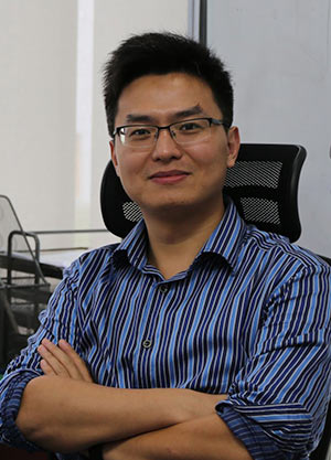
Gan Wang Assistant Professor
email: wangg@sustech.edu.cn
Office:Room 229, Research Building 2
Research Field:Molecular Beam Epitaxy、Synthesis of 1D semi-conductor nanostructures、Physics of Bismuth based topological insulators
Essential Information
Name: WANG Gan
Position: Assistant Professor
Highest Degree:PhD in Nano Science and Technology, The Hong Kong University of Science and Technology
Telephone(office):0755-88018216
Office:Room 229, Faculty Research Building 2
Email:wangg@sustc.edu.cn
Research Field:
◆Molecular Beam Epitaxy
◆ Synthesis of 1D semi-conductor nanostructures
◆Physics of Bismuth based topological insulators
Educational Background
◆ Ph.D., in Nano Science and Technology, The Hong Kong University of Science and Technology, 2011;
◆ B.S., in Condensed Matter Physics, University of Science and Technology of China, 2006.
Working Experience
◆ Jan 2012 - Present, Assistant Professor, Department of Physics, Southern University of Science and Technology
◆ Feb 2011 - Jan 2012, Post-doctoral Fellow, The Hong Kong University of Science and Technology.
Selected Publications
◆“Factorsaffecting the shape of MBE-grown laterally aligned Fe nanowires” Lok, S. K.Tian, J. C. Wang, Y. Lai, Y. H. Lortz, R. Petrovic, A.; Panagopoulos, C.; Wong,G. K. L. Wang, G. Sou, I. K., Nanotechnology, 23 (48), 485605(2012)
◆“ImpurityEffect on Weak Antilocalization in the Topological Insulator Bi2Te3” Hong-TaoHe, Gan Wang, Tao Zhang, Iam-Keong Sou, George K. L Wong, Jian-Nong Wang,Hai-Zhou Lu, Shun-Qing Shen, and Fu-Chun Zhang, Physical Review Letters,106(16), 166805(2011)
◆“Ni3Se4/ZnSeHeterostructured Nanowires Grown by Molecular Beam Epitaxy” Gan Wang, Shu KinLok, George K.L. Wong, and Iam Keong Sou, Small, 7(11), 1546–1551(2011)
◆“ZnSeNanotrenches: Formation Mechanism and Its role as a 1D Template” Gan Wang, ShuKin Lok, and Iam Keong Sou, Nanoscale Research Letters, 6, 272(2011)
◆“MBE-GrownII–VI and Related Nanostructures” Iam Keong Sou, Shu Kin Lok, Gan Wang, NingWang, and George K. L. Wong, Journal of Electronic Materials, 39(7),882-892(2010)
◆“MolecularBeam Epitaxy-Grown Bi4Te3 Nanowires” Gan Wang, Shu Kin Lok, George K.L. Wong,and Iam Keong Sou, Applied Physics Letters, 95, 263102(2009)
◆“TheFormation of an Aligned 1D Nanostructure on Annealed Fe/ZnSe Bilayers” GanWang, Shu Kin Lok, Siu Keung Chan, Chao Wang, George K.L. Wong , Iam Keong Sou,Nanotechnology, 20 (21), 215607(2009)
◆“GrowthTemperature Dependence of the Structural and Photoluminescence Properties of MBE-Grown ZnS Nanowires” ShuKin Lok, Gan Wang, Yuan Cai, Ning Wang, Yong Chun Zhong, Kam Sing Wong, and IamKeong Sou, Journal of Crystal Growth, 311 (9), 2630-2634(2009)
◆“Fe-Layer-InducedAligned 1D Nanostructure on ZnSe Surface” Gan Wang, Shu Kin Lok, Siu KeungChan, Chao Wang, George K.L. Wong, and Iam Keong Sou, Journal of CrystalGrowth, 311 (7), 2205-2207(2009)
◆“NanotrenchesInduced by Catalyst Particles on ZnSe Surface” Siu Keung Chan, Shu Kin Lok, GanWang, Yuan Cai, Ning Wang, and Iam Keong Sou, Journal of Electronic Materials,37 (9), 1344-1348(2008)
◆“MBE-GrownCubic ZnS Nanowires”Siu Keung Chan, Shu Kin Lok, Gan Wang, Yuan Cai, Ning Wang,Kam Sing Wong, and Iam Keong Sou, Journal of Electronic Materials, 37 (9),1433-1437(2008)
◆“FormationMechanism of Nanotrenches Induced by Mobile Catalytic Nanopartilces” Siu KeungChan, Shu Kin Lok, Gan Wang, Yuan Cai, Yong Jian Wang, Ning Wang, Iam KeongSou, Applied Physics Letters, 92(18),183102(2008)
Honors & Awards
◆ Receipt of Oversea High-Caliber Personal Award, Shenzhen
Research Project
◆ 2012, Young Science Research Project Awarded by National NaturalScience Fundation of China (NSFC), Principal Investigator (PI).


